Hardware and Embedded Systems
|
|
How
I designed the first Australian SPARC
Workstation
|
|
Texas
Instruments
TI-58C
Powered
By
USB 
|
|
|
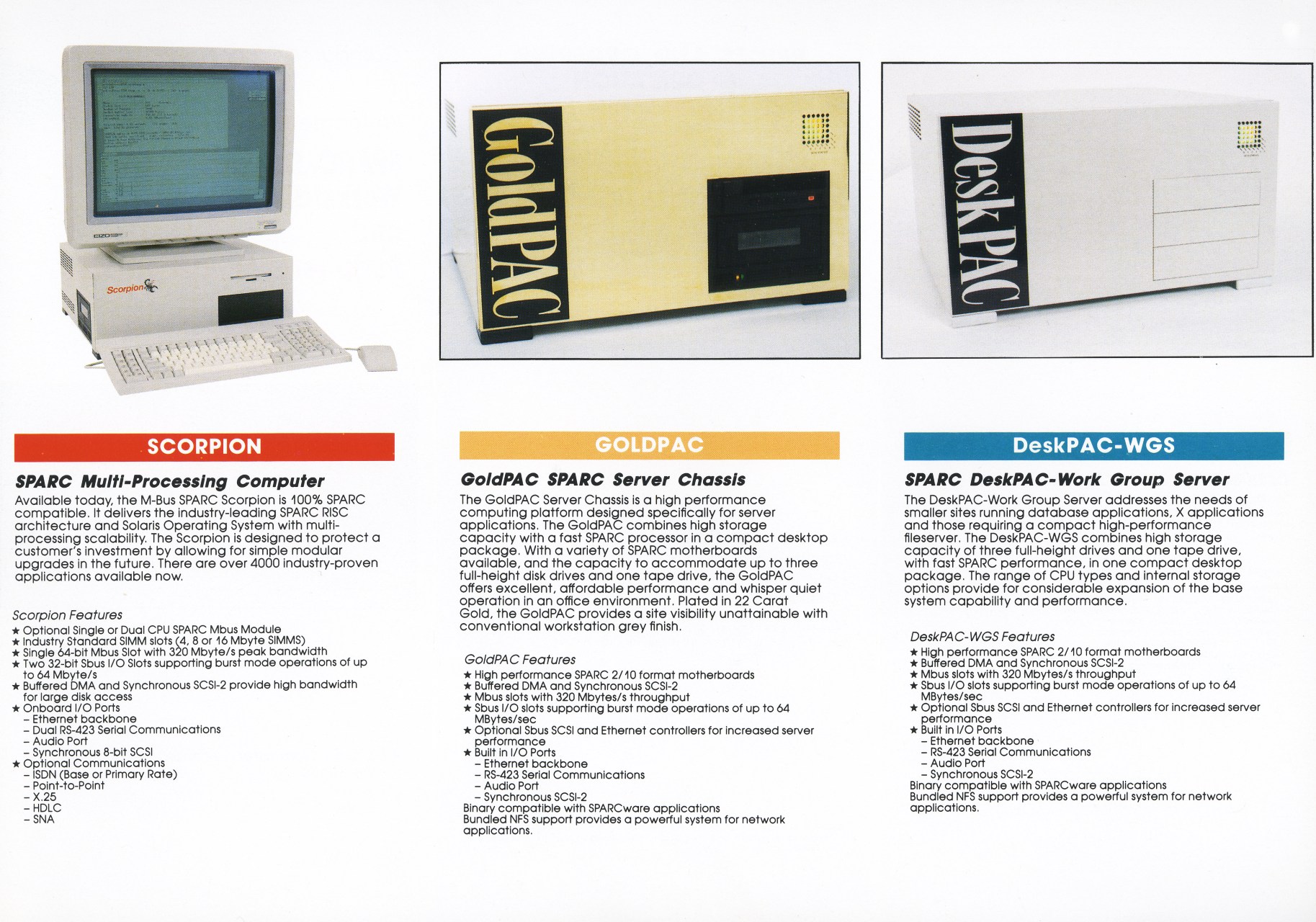
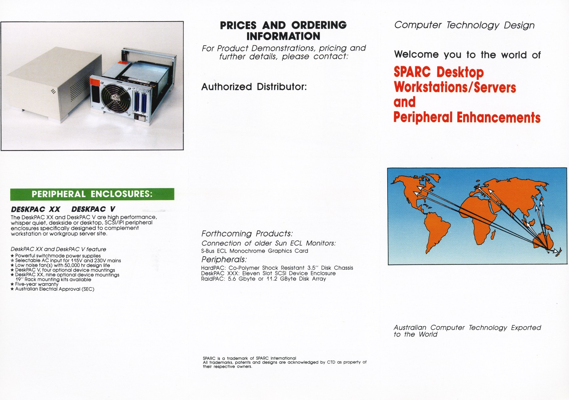
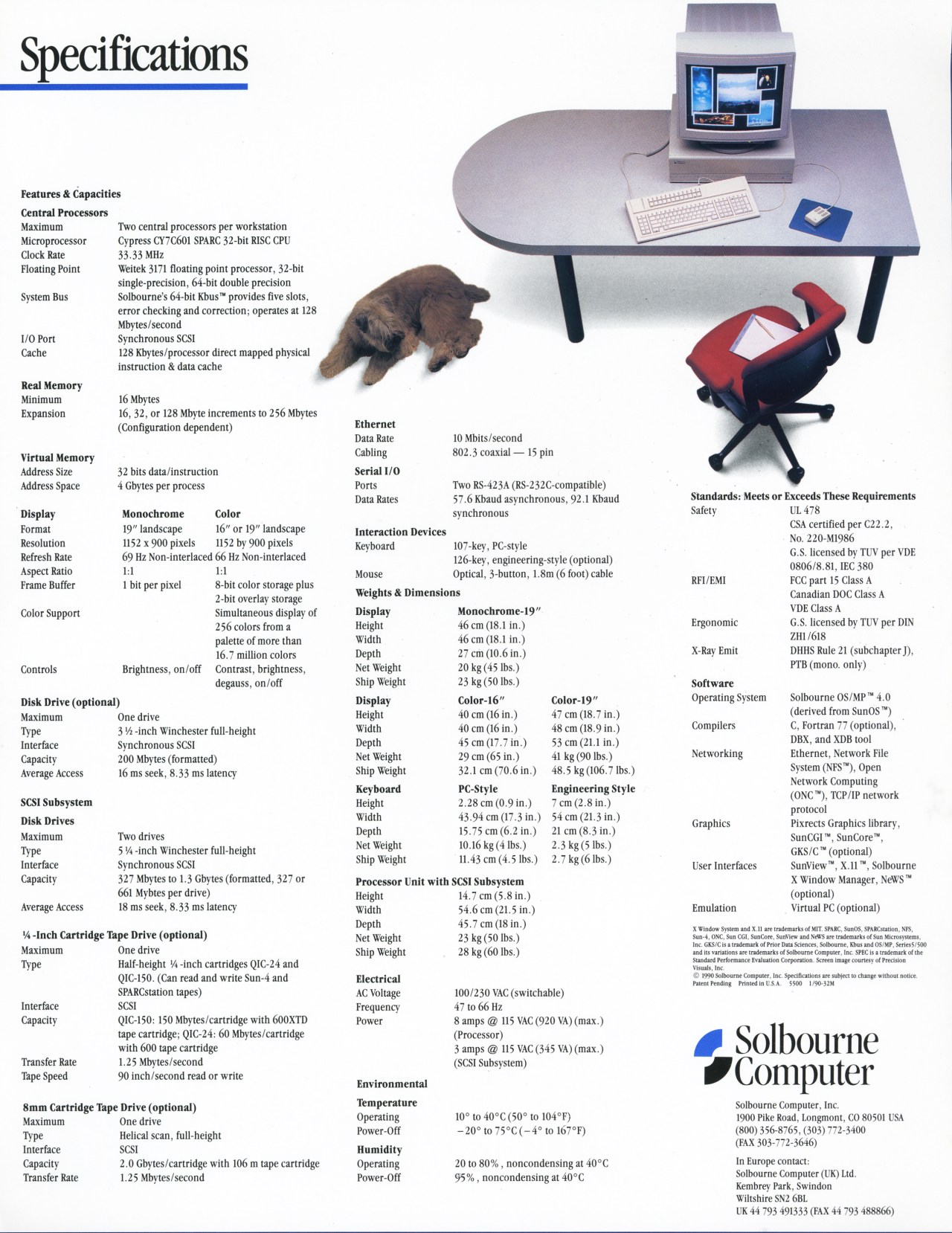
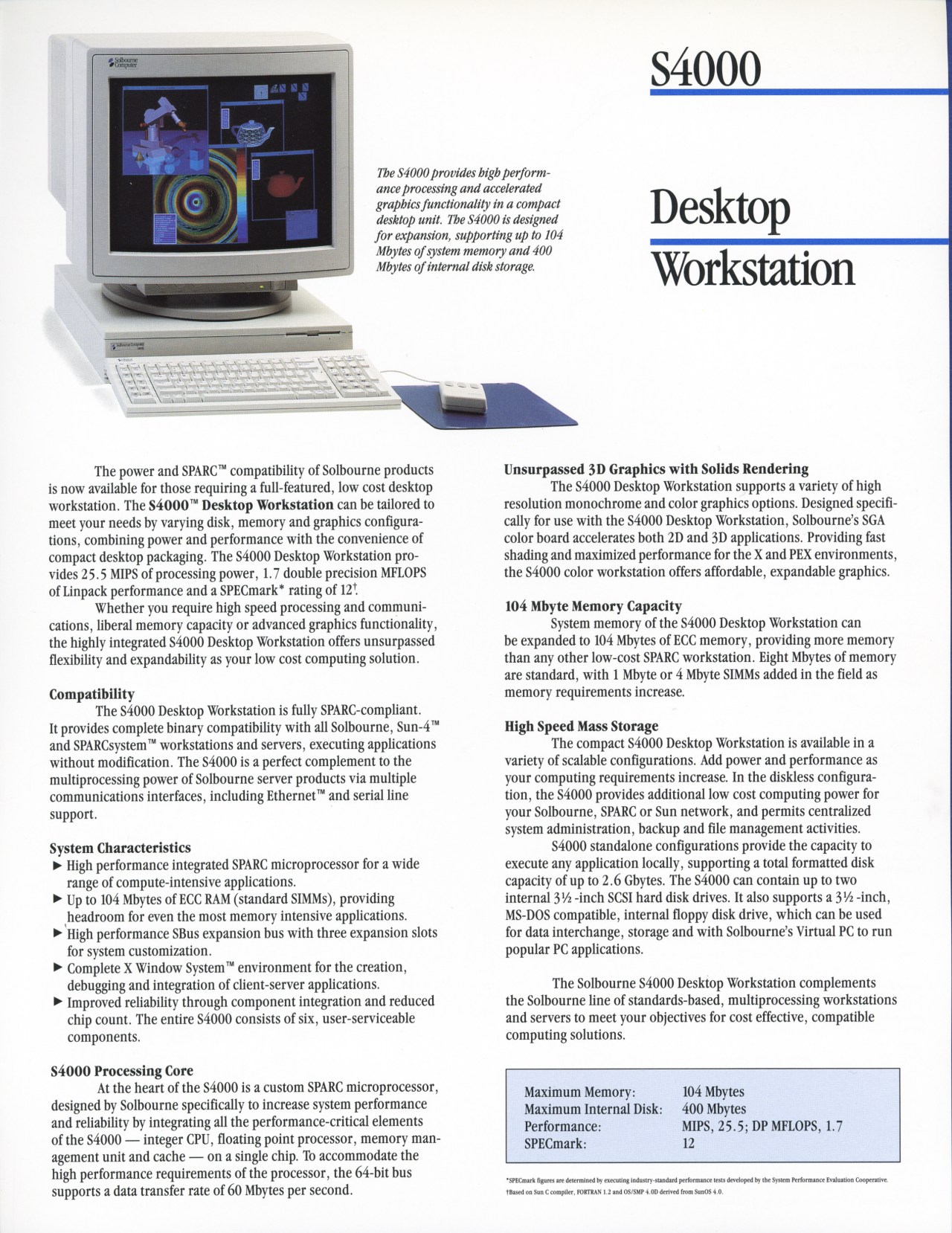
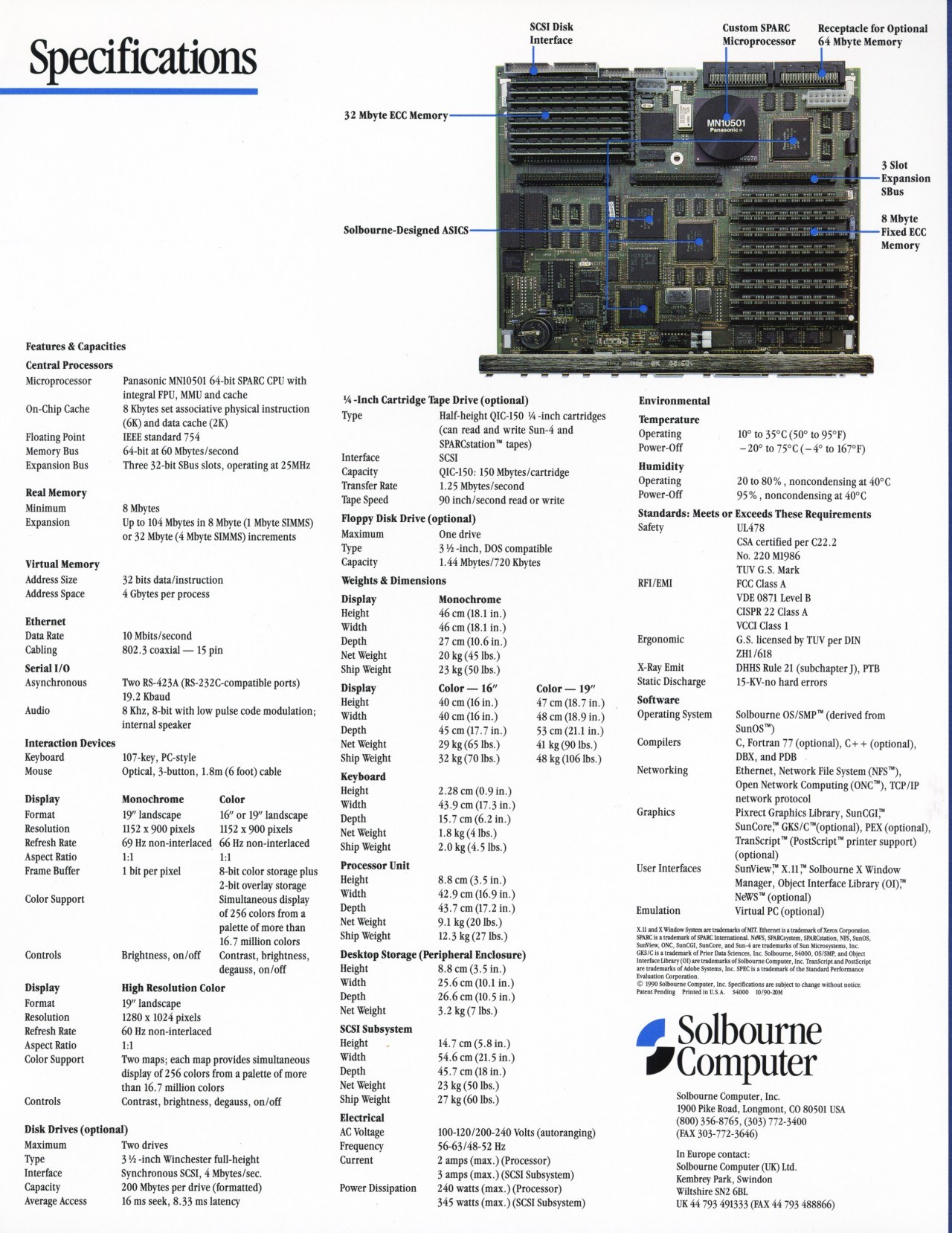
Product Design Notes, Brochures and Documentation
|
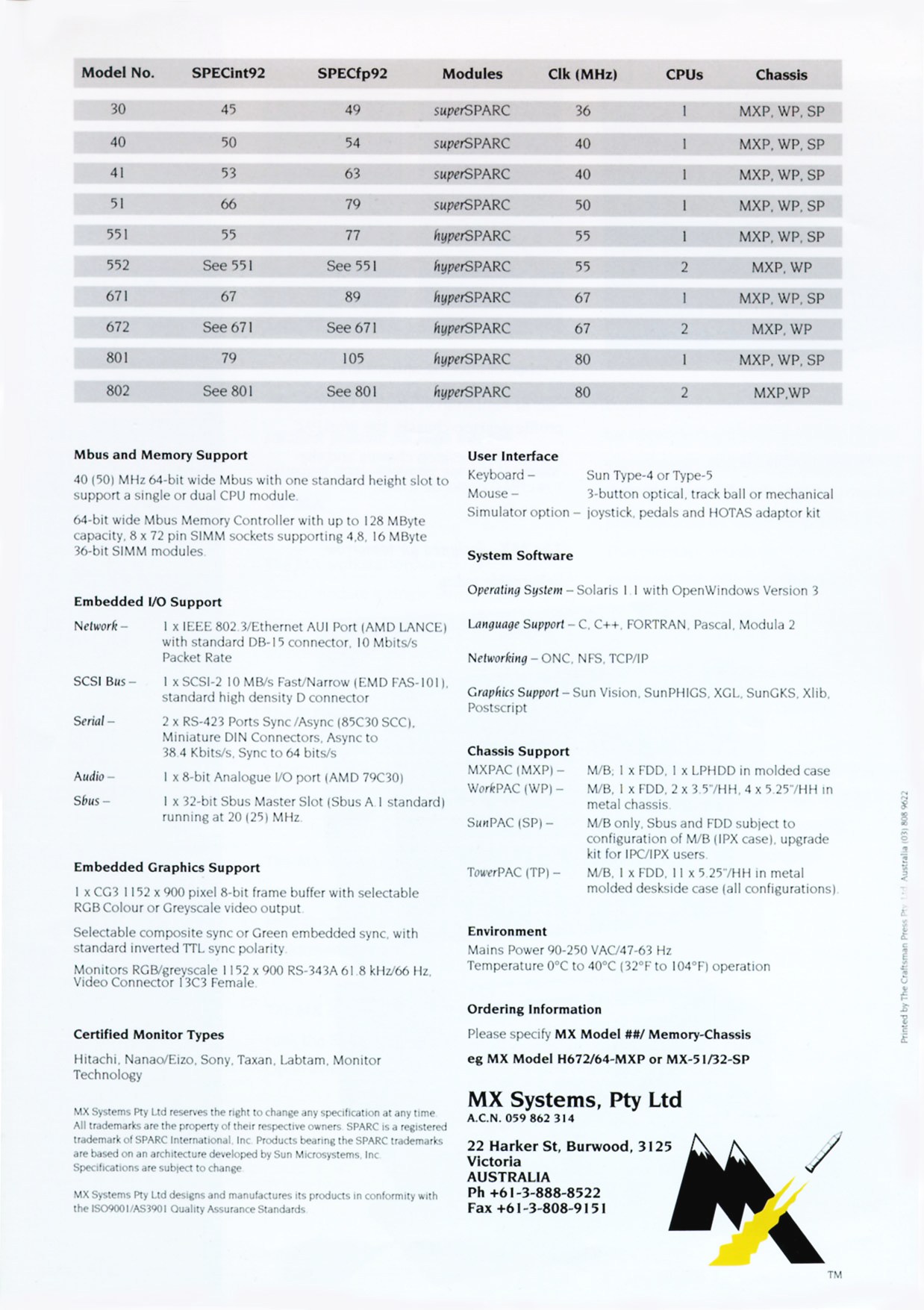
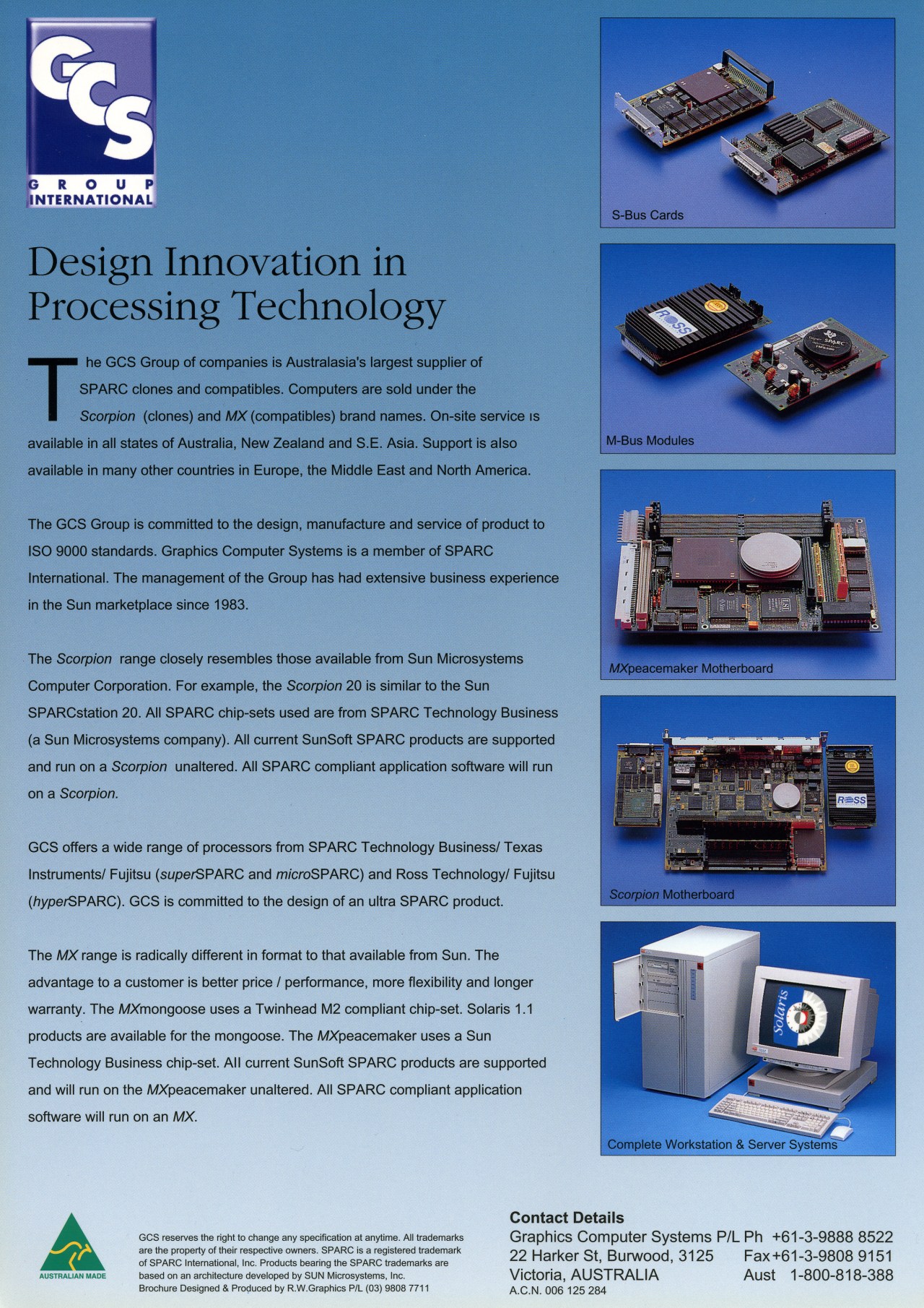
| GCS/CTD
Product
Line
Brochure
- Front Page - Rear Page |
|
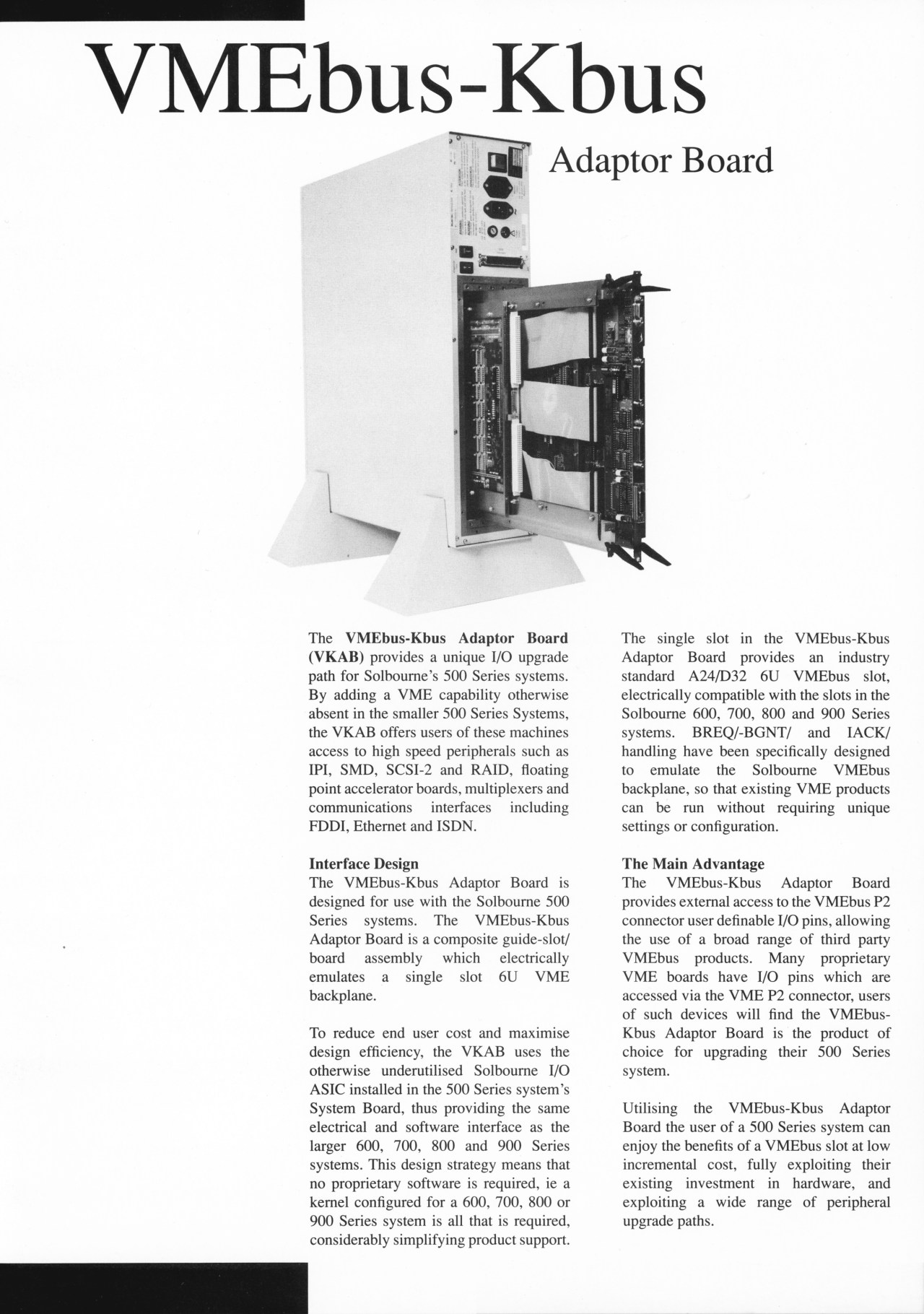
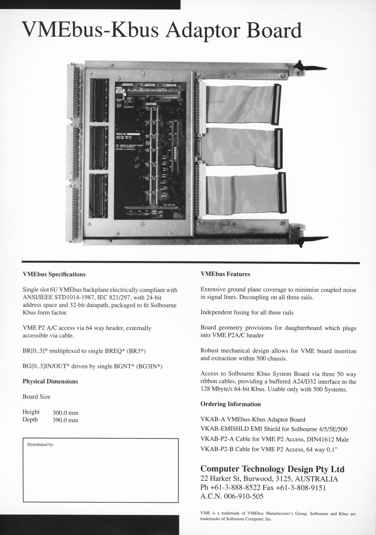
Solbourne VKAB K-bus to
VME-bus
Adaptor
Computer Technology Design / Graphics Computer Systems, 1992
|

|

|
|
Depicted
here
slotted
into
a
Solbourne
S5/500
chassis, this adaptor was designed to accommodate 6U VME boards in the
"VME-less" narrow profile chassis. This product never made it beyond
the
prototype stage. The launch customer changed their mind about what they
wanted. 100% basic hardware and mechanical design. The RHS image shows
an installed 6U VME Ethernet adaptor, and the internal K-bus I/O board
of the Solbourne which included serial ports, console port, monochrome
frame buffer, and Ethernet AUI port.
In
a
subsequent
project
I
ported
an
SS1+
synchronous
HDLC
serial
port
driver
(zs()
device
-
Zilog
8530 SCC) to the I/O board, which also
required 'stitching' additional clock lines on to serial ports (and
glueing in extra RS-232C I/O chips). Some idiosyncrasies of the OS/MP
kernel made this an interesting exercise. I later ported this driver to
the S4000 motherboard running OS/MP 4.0.
A
related
VME
project
which
migrated
to
the
Sun
4/260
was
modification
of
the
existing
port
of
the CMC-1800 ISDN Primary Rate (30B+D) 6U VME card
driver, which required the addition of diagnostics into the probe()
code.
Perhaps
the
most
disappointing
project
I
started
during
the
GCS/Solbourne
VME
era
was
the
intended
port
of
the Sun 4/260 channel adaptor for the CRAY
supercomputer, replacing the 4/260 with a Solbourne S5/600. After being
told I had the project as lead engineer and would be doing the
port and integration work, the customer balked at the last moment and
bailed out. That was my nearest close encounter with the supercomputing
hardware world.
|
|
MX
Mongoose Type C Alpha 0, SPARC
Motherboard
Computer Technology Design /
Graphics Computer Systems, 1992
|
Brochure
for MX
SPARC
Workstation
(Mongoose)
Front Page - Inner Left Page - Inner Right Page - Rear Page
|
|
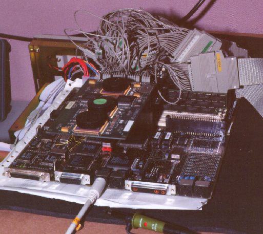
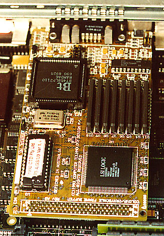
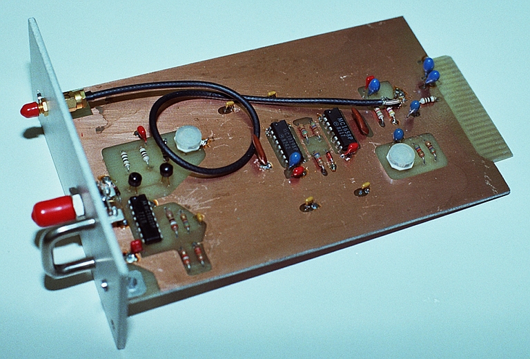
Two images here
depict the
first prototype of the Mongoose SPARC motherboard, a single M-bus,
single S-bus slot IPC/IPX form factor workstation motherboard. This
design is the first ever Unix workstation to be commercially
manufactured in Australia, and the first ever SPARC workstation design
Down Under.
I produced the
prototypes in cca 6 months from starting,
and
took about 2-3 months to debug to an early production standard. Cables
hanging off the CYM-6002K-40 CPU module belong to the HP-1651 Logic
Analyser used during the debug. CPU and Mbus clock speed of this board
was 40 MHz.
|
|
 |
The
most
difficult
problem
we
had
to
grapple
with
during
the
debugging
was
a
sensitivity to clock
skew in the motherboard chipset. This skew sensitivity was later found
to be the result of chipset documentation errors which led to incorrect
support circuitry designed around the the IC. Not our fault, but it
caused us much pain before it was isolated and fixed. |
|
|
|

|
The
upper image is the Alpha 0 motherboard blank.
|
|
|
|
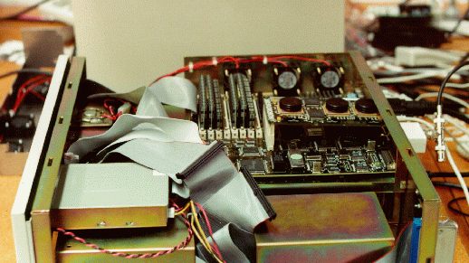
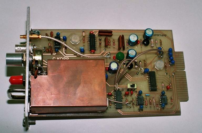
The third Mongoose
image
depicts a prototype in late debug, fitted to a Mongoose specific fan
and
mounting tray in a CTD WorkPAC chassis, also a design of mine. Note the
requirement for high airflow over the CPU dictates the use of a lateral
array of fans, and interesting design problem in its own right. The PCB
has eight layers and in its time it was the largest and most complex
PCB
in its class ever built in Australia.
|
Note that
this example
has the Sbus CG3 embedded frame buffer loaded, unlike the earlier
prototype. The design is characteristic of the transitional period
between pure surface mounted and pure conventional IC packaging. A mix
of packages is used, with PALs, NVRAM, EPROMs all in conventional
standard pitch sockets. Baseline project 100% hardware plus some of the
SunOS drivers, and regression testing of SunOS port. |
|
|
|
|
dmesg trace for
Mongoose C
VAC
ENABLED
in
COPYBACK
mode
SunOS
Release
4.1.3
(MONGOOSE)
#2:
Mon
Dec
8
16:28:31
EST
2003
Copyright
(c)
1983-1992,
Sun
Microsystems,
Inc.
cpu
=
GCS,MX10
mod0
=
Ross,RT625
(mid
=
8)
mem
=
65120K
(0x3f98000)
avail
mem
=
61022208
cpu0
at
Mbus
0x8
0x220000
entering
uniprocessor
mode
Ethernet
address
=
0:41:47:ee:0:1d
espdma0
at
SBus
slot
0
0x400000
esp0
at
SBus
slot
0
0x800000
pri
5
(sbus
level
3)
sd0
at
esp0
target
3
lun
0
sd0:
<Quantum
Atlas
V
QM309100XCLW
cyl
9004
alt
2
hd
8
sec
246>
sd2
at
esp0
target
2
lun
0
sd2:
<DCAS-34330
cyl
8203
alt
2
hd
6
sec
171>
st0
at
esp0
target
4
lun
0
st0:
<Exabyte
EXB-8505
8mm
Helical
Scan>
ledma0
at
SBus
slot
0
0x400010
le0
at
SBus
slot
0
0xc00000
pri
7
(sbus
level
4)
cgthree0
at
SBus
slot
2
0x0
pri
9
(sbus
level
5)
zs0
at
sys
0xf0200000
pri
12
(onboard)
zs1
at
sys
0xf0100000
pri
12
(onboard)
SUNW,fdtwo0
at
sys
0xf0900000
pri
11
(onboard)
audio0
at
sys
0xf0400000
pri
13
(onboard)
MBus
clock
frequency
=
40Mhz
root
on
sd0a
fstype
4.2
swap
on
sd0b
fstype
spec
size
251904K
dump
on
sd0b
fstype
spec
size
251892K
|
 |
|
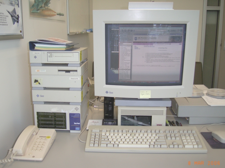
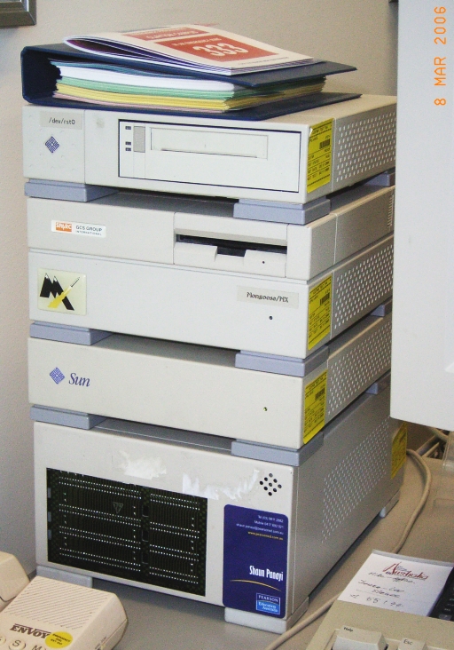
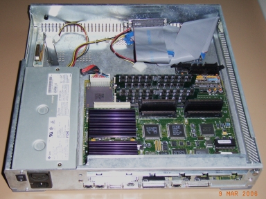
The Last
Mongoose?
Above and right: Mongoose C
preproduction
motherboard S/N 0009 (1994) remained in service primarily as an
Xterminal (with
8-bit colour only unfortunately), running as intended in a Sun IPC
chassis. The motherboard was loaded in Australia, the PCB made in
Silicon Valley.
This system was donated to me by GCS in 1996, and remained in
service continuously until 2008, when it was no longer capable of
properly supporting the bandwidth of more demanding X11 applications.
It is loaded with a 90 MHz HyperSPARC, 64 MB of DRAM and a Quantum
Atlas V internal hard disk, with a 4 GB BM external disk and an
Exabyte EXB-8505 tape. Note the original GCS badges on the chassis.
Over its extended operational life it has outlasted two internal SCSI
hard drives,
both of which failed due to the relatively high internal temperature in
the Sun IPC chassis, not designed to be hard disk friendly.
The chassis below the stack is a Trimm
Industries 5.25" enclosure, the
chassis below the monitor is a Digital Equipment Corp badged Trimm
Chassis, with DEC specific ABS molded front panel.
|
|
The photographs were taken early March, 2006. As I have spare power
supplies, spare IPC chassis and other components,
this system was intended to be left operational until the motherboard
failed, as an experiment to determine the longevity of this generation
of hardware. While the main imperative in terminating the experiment
was operational, I decided that having a live Mongoose in storage was
better than having a dead one on display.
|
|
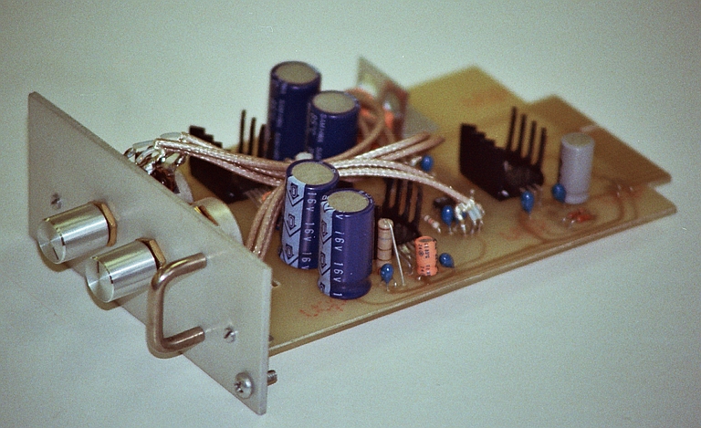
Sbus CG3 Colour Frame Buffer
Computer Technology Design / Graphics
Computer Systems, 1992
|
|
|
The Frame Buffer board depicted
here was an enhanced clone of
the standard CG3 board. In this instance I added a clever jumperable
arrangement to select true greyscale video, or standard RGB video,
using a network of mixing resistors. This meant that the board would
provide true greyscale rather than "stunted" (green only) greyscale
video when connected to the the standard SMI monochrome SS1 monitor, or
third party greyscale monitors. Designing the resistor network to match
impedances and provide the required mixing ratios proved most
interesting. Another little feature on this board was a jumper to
provide sync on green rather than SMI standard sync, again a feature
which came in very handy in the OEM marketplace. As the board used the
same LSI device as the vanilla CG3, this project was largely a hardware
exercise, with minimal firmware hacks.
The sibling Sbus BW2 clone board which I produced
earlier required more
substantial changes as I had to generate ECL video with Sun-3
compatible timing, replacing the Sun-4 video timing in the greyscale
Sbus frame buffers.
|
 |
| This
required a
substantially new board design with new Forth PROM firmware, which I
also had to produce. Without the funds to hire a logic
analyser, the
design was debugged with a 2 channel Tektronix scope. A high resolution
variant of this board, the BW2HR with 1600x1280 resolution, never got
past the paper design phase, the hi-res 1600x1280 CG6 derivative, and a
CG8 derivative also never made it. Related products included a
multiport
ECL video driver box for testing monitors. |
|
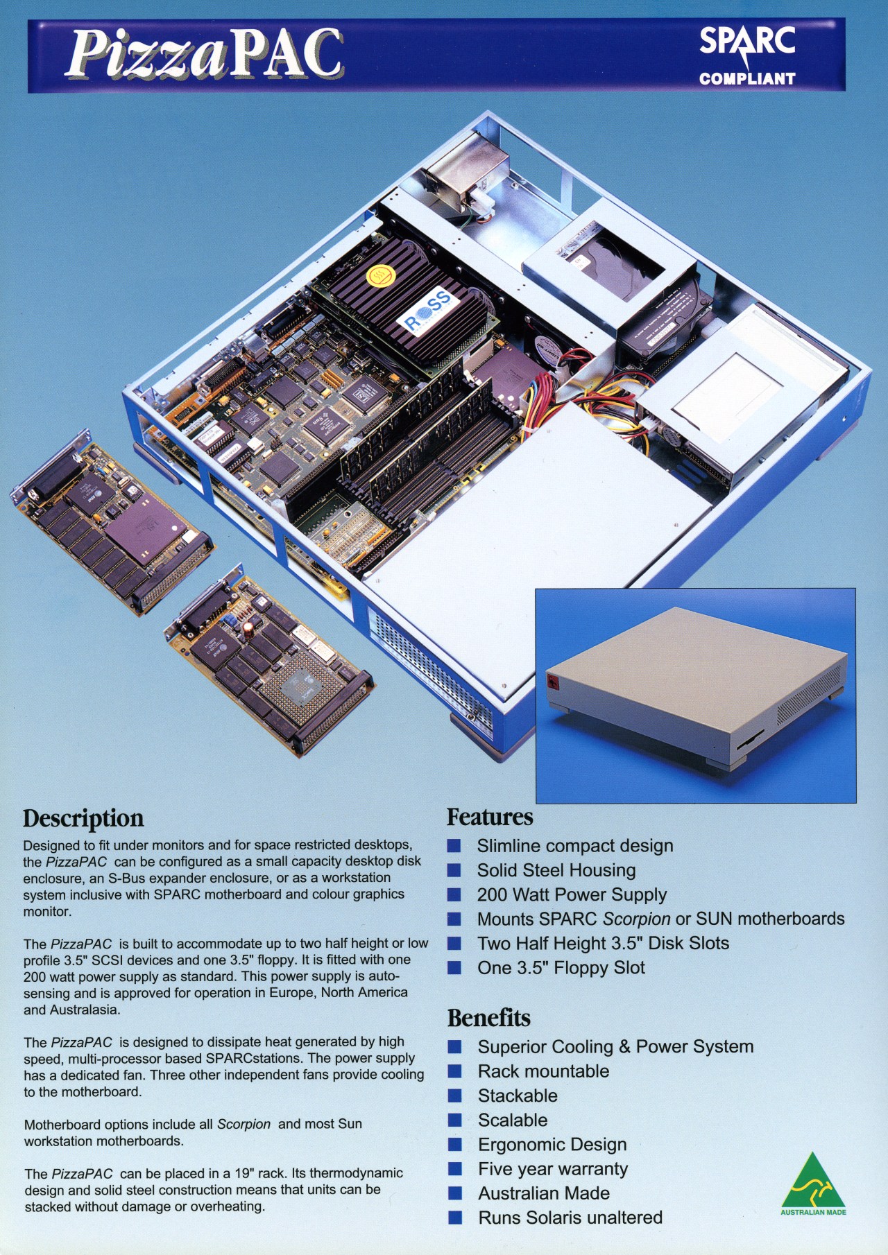
PizzaPAC
SPARC
Workstation
Computer Technology Design / Graphics Computer Systems,
1992
|
|
 |
The
'PizzaPAC' marketing label was used for a range of 'pizzabox' desktop
systems, using Twinhead or Integrix supplied motherboards and imported
chassis. This example is an SS10 system using an Integrix chassis and
motherboard, with a HyperSPARC CPU loaded. The Scorpion badge was
created by graphic artist Mark Kopp (my since deceased youngest
brother) in Perth.
|
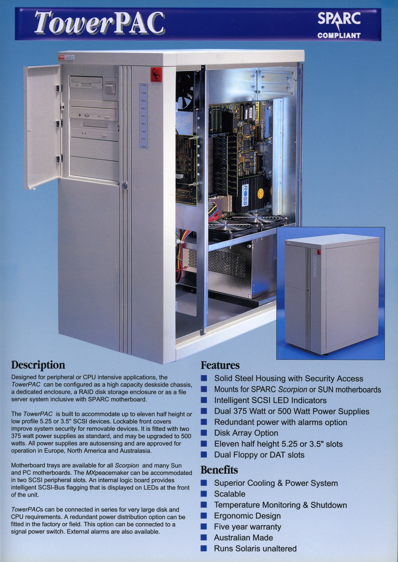
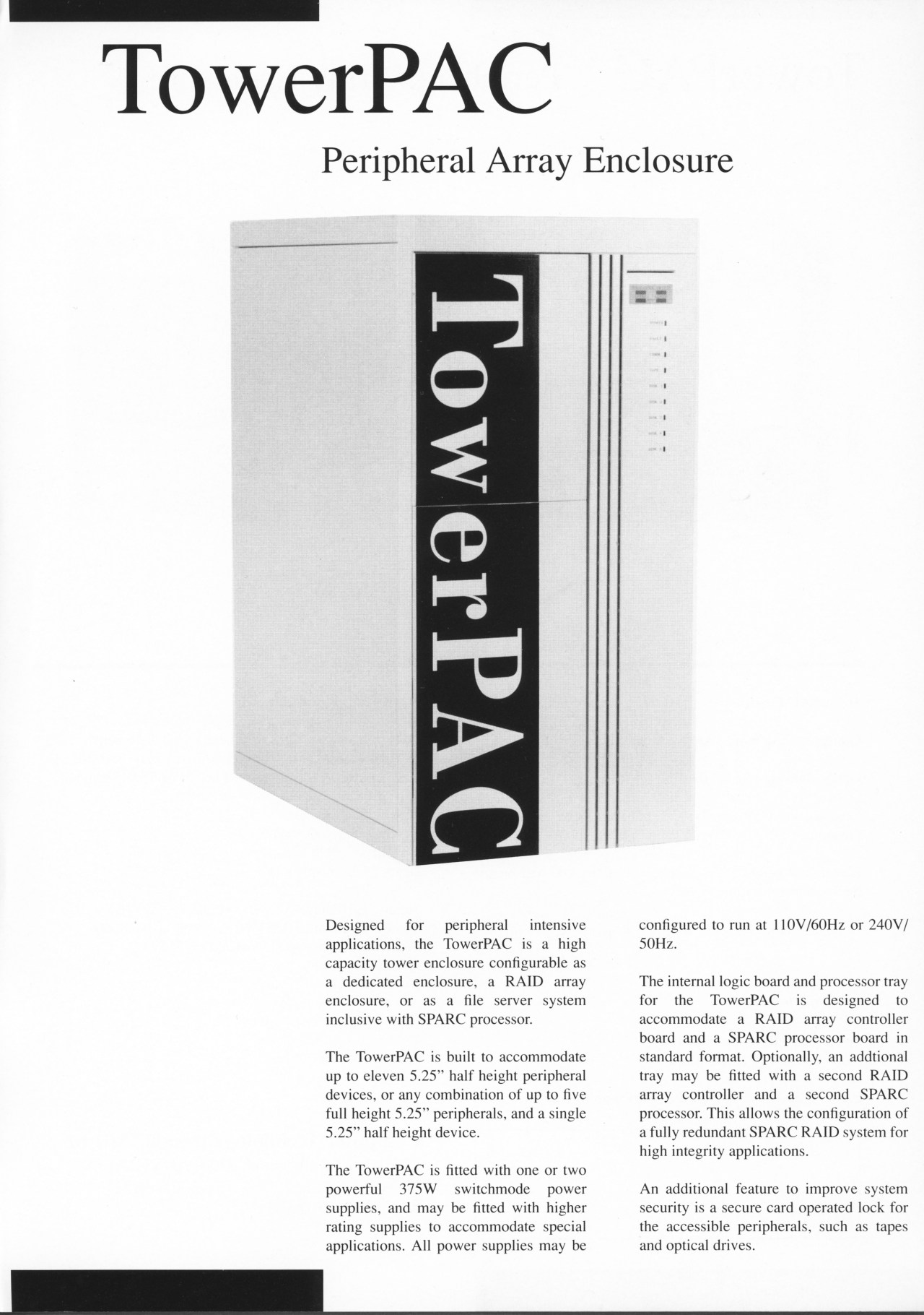
TowerPAC SPARC Server
Computer Technology Design / Graphics Computer Systems,
1992
Brochure for TowerPAC
Peripheral/Server
Chassis
Front Page - Rear Page - (internal metalwork
design only)
The TowerPAC was an imported
Taiwanese built Server case which GCS adapted by installing an CNC
punched and folded internal tray designed to accommodate the SS10 or
later SS20 motherboard. The tray also mounted a pair of low RPM 120 mm
fans to blow airflow over the motherboard, while also including
mounting holes for additional SCSI connectors.
The TowerPAC's debut was comical. The MD, Geoff Croker, forgot to
notify me that he intended to sell this product and sold the first unit
while my engineering office remained blissfully unaware of the
impending embarrassment. The CPU tray was designed, the prototype
delivered, tested, installed and shipped to the client in three days. A
very hectic three days, suffice to say. In hindsight the TowerPAC had
the shortest gestation and development cycle of any product I had ever
worked on. Note the small PCB on the SCSI connector, this was an
adapter we designed which included SCSI terminators and a 0.1" pitch
header for standard low density cable use.
The depicted example has a dual CPU HyperSPARC loaded, and a GCS built
CG3 Sbus frame buffer.
|
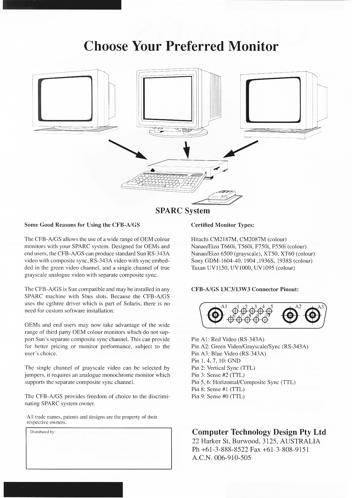
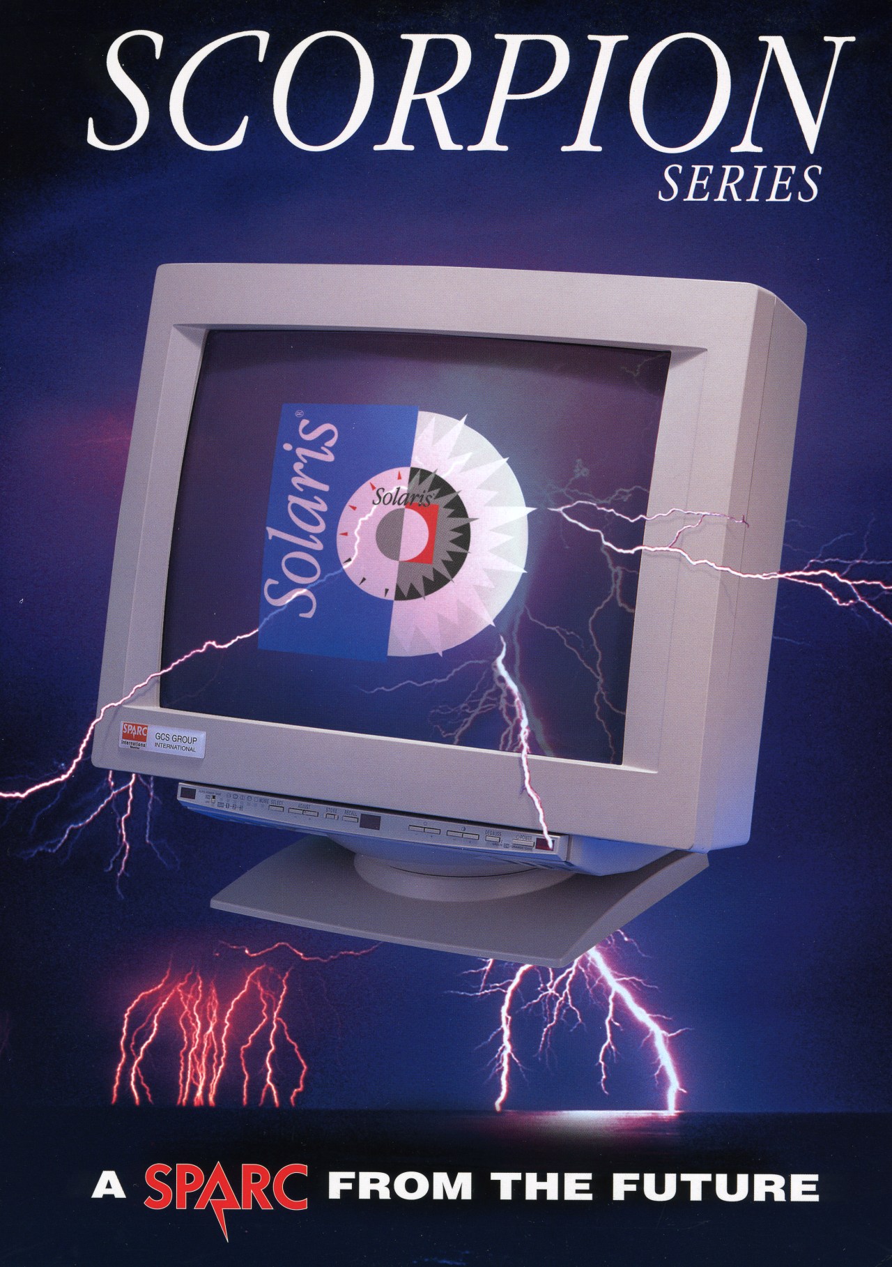
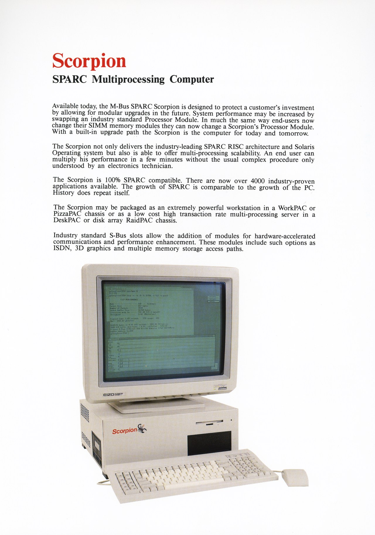
Scorpion / WorkPAC Server /
Peripheral Enclosure
Computer Technology Design / Graphics Computer
Systems, 1992

|
|
Brochure for Scorpion
System
(Twinhead
M/B)
- Front Page - Rear Page - (WorkPAC chassis
design)
These two chassis were designed
as OEM
enclosures for SPARC workstations and associated peripherals. Probably
the most important design feature in these products was the use of
large
low RPM fans to provide extra airflow for poorly air conditioned office
environments, and low fan noise. Both were manufactured in Melbourne.
The fishtank image on the monitor is the real
thing, we built a fish tank into the carcass (case) of a dead RGB
monitor.
|
|
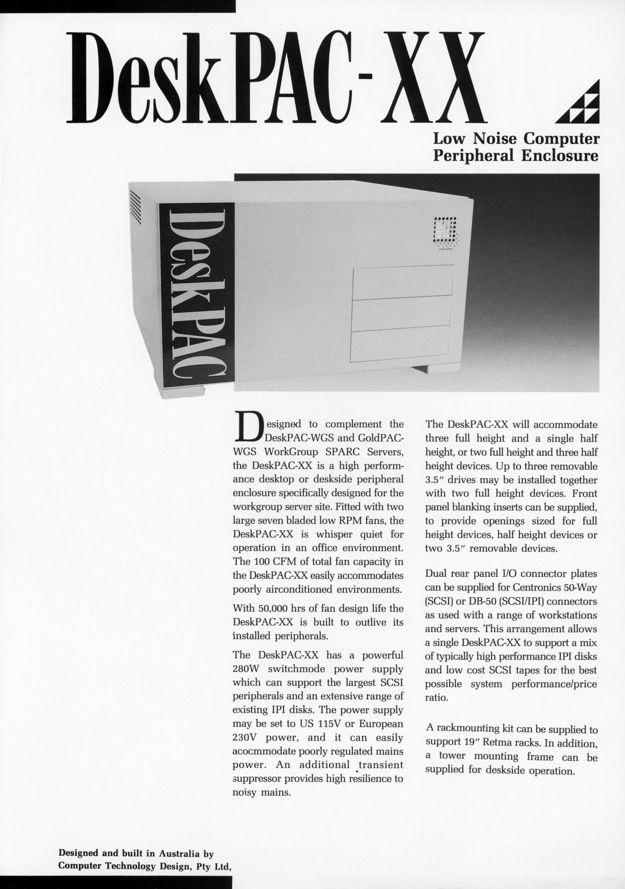
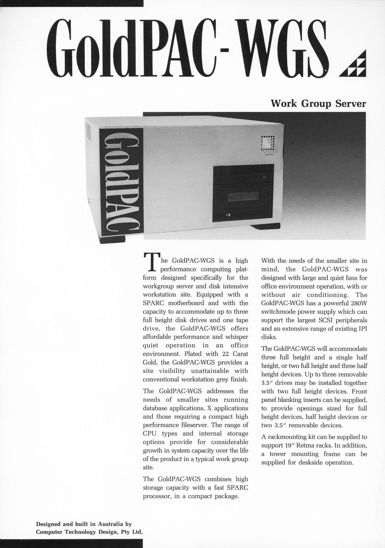
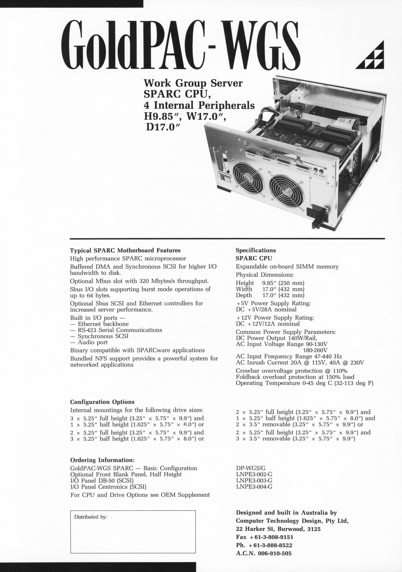
DeskPAC-20 Server / Peripheral
Enclosure
Computer Technology Design / Graphics Computer Systems,
1992
|

|

|
The DP-20 was used
both
as a peripheral chassis but also as a server chassis, with an installed
CPU tray, unique to the motherboard used. DP-20s were used for the SS2,
Mongoose C and SS-10 motherboards. Internal brackets permitted the
installation of up to three 5.25" full height drives, two being
installed at 90 degrees to the base of the chassis. Production
quantities of the DP-20 ran into hundreds over several years. Variants included a stainless
steel model, and a 22-carat gold plated
model (which sold quite well - mostly to public service clientele!).
|
|
DeskPAC-5 5.25 inch Peripheral
Enclosure
Computer Technology Design / Graphics Computer Systems, 1992
|

|

|
|
Curiously, of all of
my
product designs, the DeskPAC-5 'shoebox' remained in production the
longest, being built for at least seven years. Designed initially to
reliably support the hot running Seagate Elite-9 5.25" drive in poorly
airconditioned environments, the DP-5 proved to be very popular and was
built in many variants. The final and most numerous variant, the
'Rev.EA' model, was optimised for minimal metalwork production cost,
minimising the number of folds and punched holes in the metalwork, but
also using improved internal airflow routing to maximise cooling
effect.
Designing good chassis can be challenging as it amounts to an 'origami
game' in devising clever strategies to build up the box from as few
parts as possible, with a minimal number of CNC operations per part.
|
|
|
32 Mbits/s High Speed
Optical
Datalink (HS-ODL)
Dataplex Pty Ltd, 1989
Following
the
completion
of the DPX-610 my subsequent project was the later abandoned
32 Megabit/s rooftop optical datalink. At that time DPX manufactured a
highly successful product line of low cost optical links, used to
connect LANs between buildings up to 1 kilometre distant, at speeds up
to 2 Mbits/s. The 'high speed ODL' was to extend the range and speed of
the product line, and was an entirely new design using the telescope
assemblies of the earlier product. This design reached the point of PCB
layout but was shelved. Packaged on circular PCBs, the HS-ODL used a
differential pair laser driver cascaded from a differential ECL buffer
stage, and a variant of the low noise receiver used in the UWA optical
link. The design included an infrared filter window using rare earth
doped glass, with a multilayer bandpass interference filter, a measure
necessary to cope with the background current arising from solar
illumination - much the same design problem faced by designers of
heat-seeking missiles. Unlike thermal dark current in fibre receiver
detectors, background current can be a crippling source of shot noise
in
free space optical links. No material documenting this project has
survived, unfortunately.
|
DPX-610 K-Mux Medium Speed
Synchronous Mux
Dataplex Pty Ltd, 1989

")
")
|
|
The K-mux was my last
and most
complex communications equipment design, which absorbed much of my
effort over an 18 month period. This design used no less than five
Z-180
CPUs, and a pair of microcoded micromachines for generating framing
structures. The K-mux was a fully software programmable intelligent
synchronous mux which could independently manage its state and
configuration data. It used cca 20,000 lines of embedded C and
Assembler, which accounted for more than two thirds of the development
time expended. The K-mux used an embedded serial packet oriented
protocol scheme inspired by (read 'derived from') the DEC DDCMP
protocol, via which the master CPU issued commands and interrogated the
status of the up to four slave or datapump CPUs. One of the interesting
features of this design was the level of tuning in the datapump code,
where a single Z-180 at 8 MHz clock speed, using a pair of DMACs, was
capable of pushing 72 kbit/sec full duplex and synchronous.
Another interesting feature were the micromachines, which were loaded
at
boot or restart time with microcode which had been generated on-the-fly
from decoded configuration tables in non-volatile RAM. Expansion I/O
(datapump) boards in the K-mux included my design for a software
programmable fractional frequency multiplier, which allowed the
software
to synthesize any frequency which was a ratio of two integers in the
multiplier's operating range (this was done with a PLL). This provided
the DPX-610 with the most flexible clocking facilities of any mux in
its
class at that time, globally. Sadly the K-mux never made it into
production as local customers preferred less sophisticated and more
expensive imports. Probably my most original from the ground up design,
and certainly the most complex logic design.
|
|

|
|
")
|
|
|
Optically Isolated RS-422 Differential
Serial Line Interface
Monash
University
Computer
Centre, 1987

|
Between
1985
and 1987 I worked for the Monash University Computer Centre (now ITS)
as a Computer
Systems Engineer, responsible for maintaining VAX-750/780 systems,
associated peripherals, and also all network installations for Clayton
campus, including the design and project management of all of the early
optical fibre links across the campus (Apollo token ring and Ethernet).
My sole hardware design during this period was a line interface device,
designed as a replacement for long haul current loop serial lines used
to access some on campus sites. The single board device used a pair of
opto-isolators, with the DTR pin powering the RS-232C receiver side,
and
a plugpack adaptor powering the line impedance matched RS-422
side. Over a dozen were hand built and used for specific links
where network access was infeasible at the time, and current loop links
too slow. The system ran up to 38.4 kbps but was usually operated at
19.2 kbps due to the propensity for XON/XOFF characters to be lost at
the higher speed due to slow interrupt service rates. No photos are
available, but I did have archived images of the VAX-780s it was used
to
connect - usually running DDCMP protocol over the link.

|
|
Type
84
140
Mbits/s 1.31 micron Optical Fibre Line Terminal and Repeater Equipment
NEC Corporation, 1984

|
In mid 1984 I
was hired by NEC Australia to participate in the design of the new
single mode fibre 140 Mbits/s line terminal and repeater
equipment
then to be supplied to Telecom Australia (Telstra). The design work was
performed during a 4 month period at the NEC Tamagawa plant in Tokyo,
located in the area adjoining the Yokohama district. I was responsible
for repackaging and adapting the existing Japanese design for the ITU
spec export 140 Mbits/s equipment, specifically working on the optical
receiver and transmitter boards. Including the line coding overhead,
the
baseband channel was clocked at 168 Mbit/s. These boards were
implemented using NEC 600 series ECL logic devices which expanded my
ECL
design experience considerably - the NEC ECL was very similar to MECL
III and delivered exceptional switching speeds. Unfortunately the end
product remained unable to meet the 'defacto Milspec airborne' thermal
environments specified by the customer, since the customer also
insisted
on convective cardcage cooling despite our repeated advice to the
contrary. The receiver used an excellent NEC designed low dark current
Ge or GaAsP avalanche diode, and NEC manufactured lasers with internal
PIN diode power output sensors. NEC lodged several Japanese patents for
circuit designs under my name at the time. Unfortunately I have
no photographs of the equipment or the cards due to company security
policy at the time. The depicted devices include 600 series ECL gates,
bipolar single and paired RF transistors used in driver stages (common
emitters in the paired device), and a JFET, all in high reliability NEC
ceramic packaging.
|
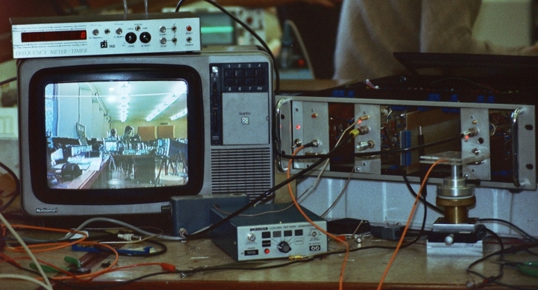
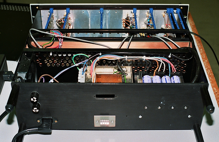
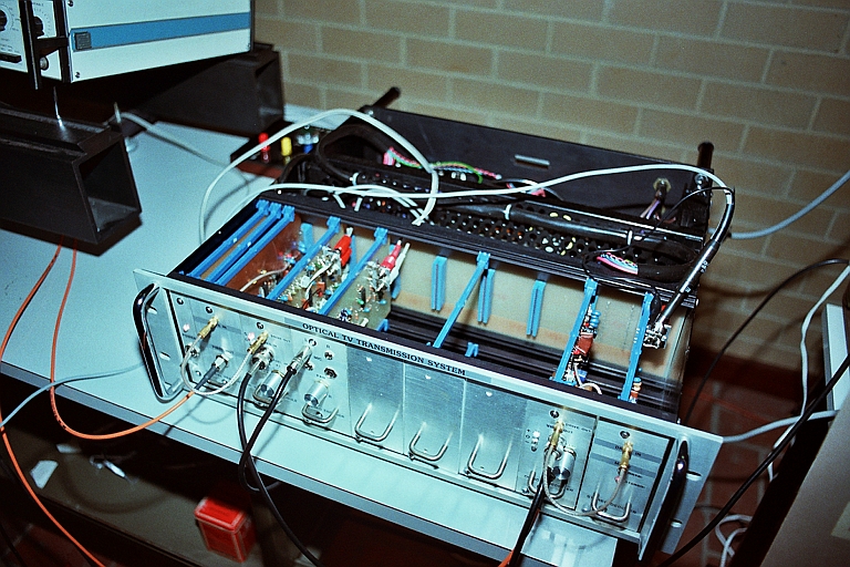
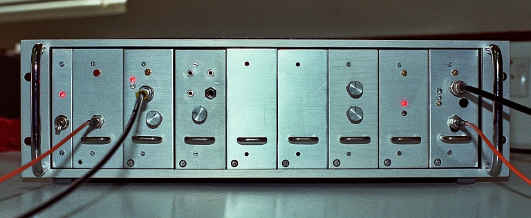
Optical
Television Transmission System (Analogue)
University of Western Australia, 1983 |
In the beginning
... My
1983 Honours project at the University of WA was my first attempt at a
major system design, in this instance wholly analogue. I was supervised
by A/Prof John Hullett, later the driving force behind the QPSX
project.
This project was also my apprenticeship as an Emitter Coupled Logic
(ECL) designer, as ECL was required in the modulator and driver stage.
The system was a Pulse Frequency Modulated design, using an MC-1658P
Voltage Controlled Oscillator, an MC-10198P monostable and an MC-10210P
as the differential pair driver for the MFOE-106F IR LED, although the
design was built to accommodate a future laser device. The low noise
wideband analogue optical receiver was derived from a UWA design used
in
OTDR equipment, and used a C30817 PIN diode and 2N4416A J-FET first
stage. The system included FM stereo encoders and decoders, an audio
amp, an FSK digital subchannel encoder/decoder and a range of other
lesser features. The design was largely 'from the ground up' including
the design of the linear power supply, system cooling and the
cardcage/chassis assembly. The following photos were recovered by
digitising archived 35 mm negatives - fortunately these survived almost
a quarter century of storage, the hardware unfortunately did not.
|
|
|
|
|
|
|
|
|
Optical
Modulator and Transmitter Module (ECL)
|
|
Low Noise
Optical Receiver and Demodulator Module
|
|
Stereo
Decoder Module
|
|
Subcarrier
Module
|
|
| Stereo
Encoder Module |
|
Audio
Amplifier Module
|
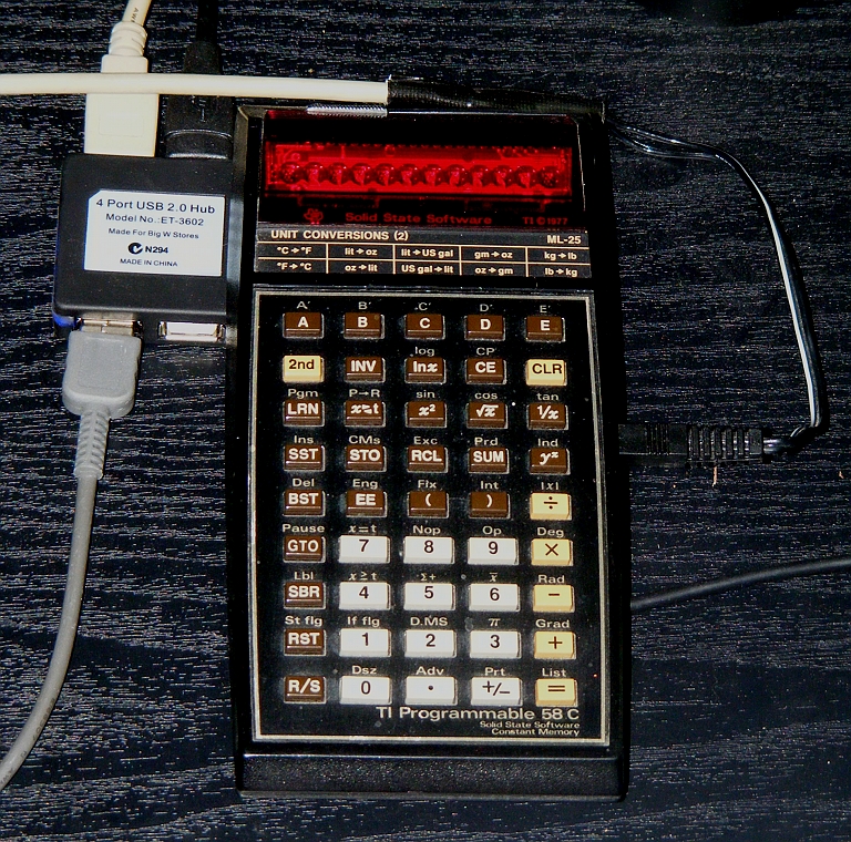
Texas
Instruments TI-58C Powered By USB
April, 2010
|
One of my
favourite computational toys is the TI-58C/59 series of handheld
calculators, which represented the state of the art around 1980. They
remain amongst the ergonomically nicest calculators ever designed, the
high contrast display being easy to read, and the keys giving the user
confidence that one digit alone was entered. The principal obstacle to
keeping the TI-58C/59 series alive is the fragile BP-1A battery pack,
which is supposed to last up to ten years. The longest any BP-1A I have
used has lasted is about 3 years. The last one I purchased was quite
expensive. So I considered the problem of how to use cheap and easily
available means to beat this problem for once and for all.
Initially I
considered rebuilding the BP-1A to use three AAA sized rechargable
batteries - elegant but time consuming and messy to implement. Ed
Grochowski, a machine architect at Intel, devised a clean
solution which exploits the fact that the TI-58C/59 series uses an
5V RMS AC power adaptor, internal rectifier, and the BP-1A as both a
battery and defacto primary charge store capacitor for the power supply
- his solution makes use of an external regulated 5VDC plugpack as a
replacement for the existing TI AC plugpack, and discards the complete
BP-1A module, plugging the hole with a plastic sheet.
Whilst I was
impressed with Ed's solution, I lacked the patience to shop around for
the required bits. This got me thinking - what is the most ubiquitous
regulated 5 VDC supply available currently? The obvious answer is the
USB which is these days used on almost everything. It took about ten
minutes to rig a prototype cable, using the power connector off a TI
plugpack, and a tatty USB 1.1 cable located at the bottom of my box of
used
cables. The installation works nicely, and the TI-58C runs much cooler
as the BP-1A is not dissipating waste heat from the charging process.
The final cable uses heatshrink tube to protect the +ve and -ve
soldered
cable splices, with additional black duct tape applied as a strain
relief,
just in case, and also protected by heatshrink. The BP-1A is gutted -
easily done by using a finely
serrated steak knife on the internal cross members retaining the three
battery cells. The total cost of the installation is negligible, unless
you choose to buy a new USB cable.
April, 2010
|
|
|
|


