a simple current source for resistance measurement
using the Kelvin Method
using the Kelvin Method
abstract
a simple 3 transistor circuit is described that implements a constant current source giving 100,50 or 20mA is described
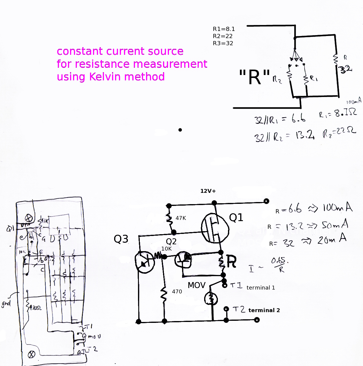
The MOV is in parallel with the output terminals. This protects the circuit from inductive surges when you are measuring the DC resistance of large inductors. Resistor R determines the value of the constant current, which is given by VbeQ1/R This circuit and the nominated resistors have been modelled in LTSPICE and in practice is found to work very well. The MOV should fire at about 30V. I used a MOV because I had one that was right, but back to back 15V Zeners would be better still.
The principle of operation:
Q1 is providing some arbitary current flow. This causes a potential differance across resistor R. If this potential is greater than VbeQ1, or about 0.6V, Q2 conducts. This adds a little forward bias to Q3 by "connecting" the base of Q3 to the high side of R. Q3 now conducts removing the positive bias on the gate of Q1, which acts to reduce the current supplied out of terminal T1. This negative feedback provides a large amount of current regulation.
The main limitation of this simple circuit is that the regulated current is programmed by Resistor R, so it is hard to adapt
to a circuit requiring variable current regulation.
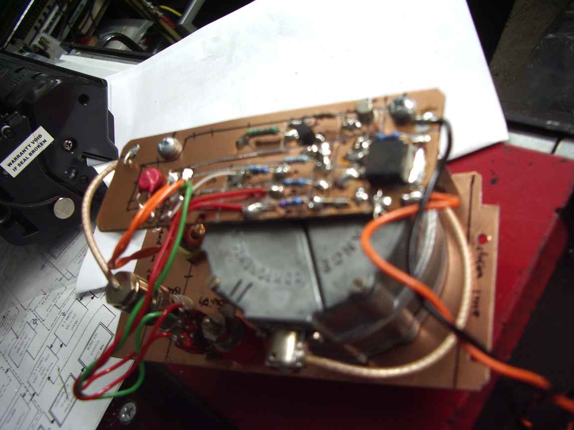
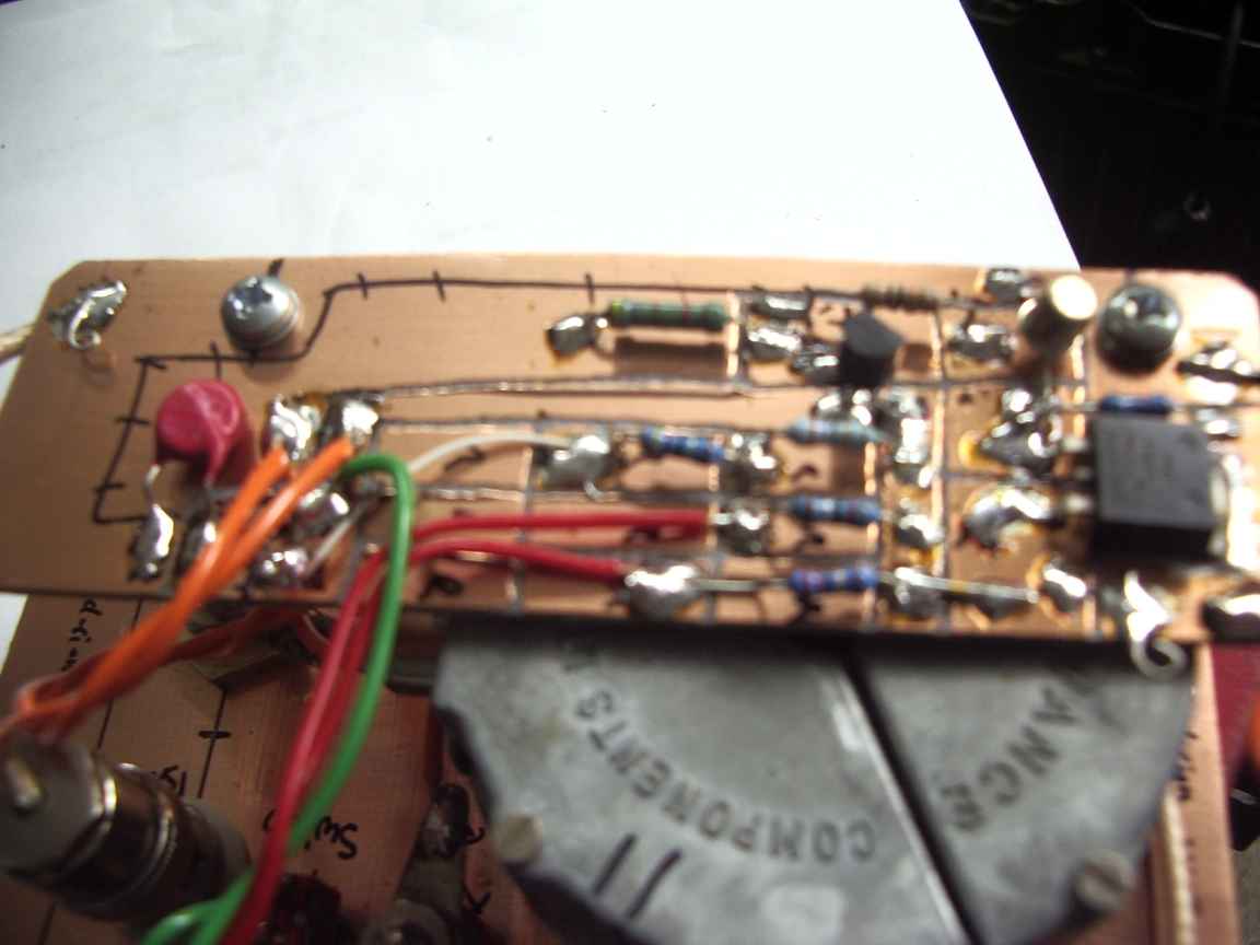
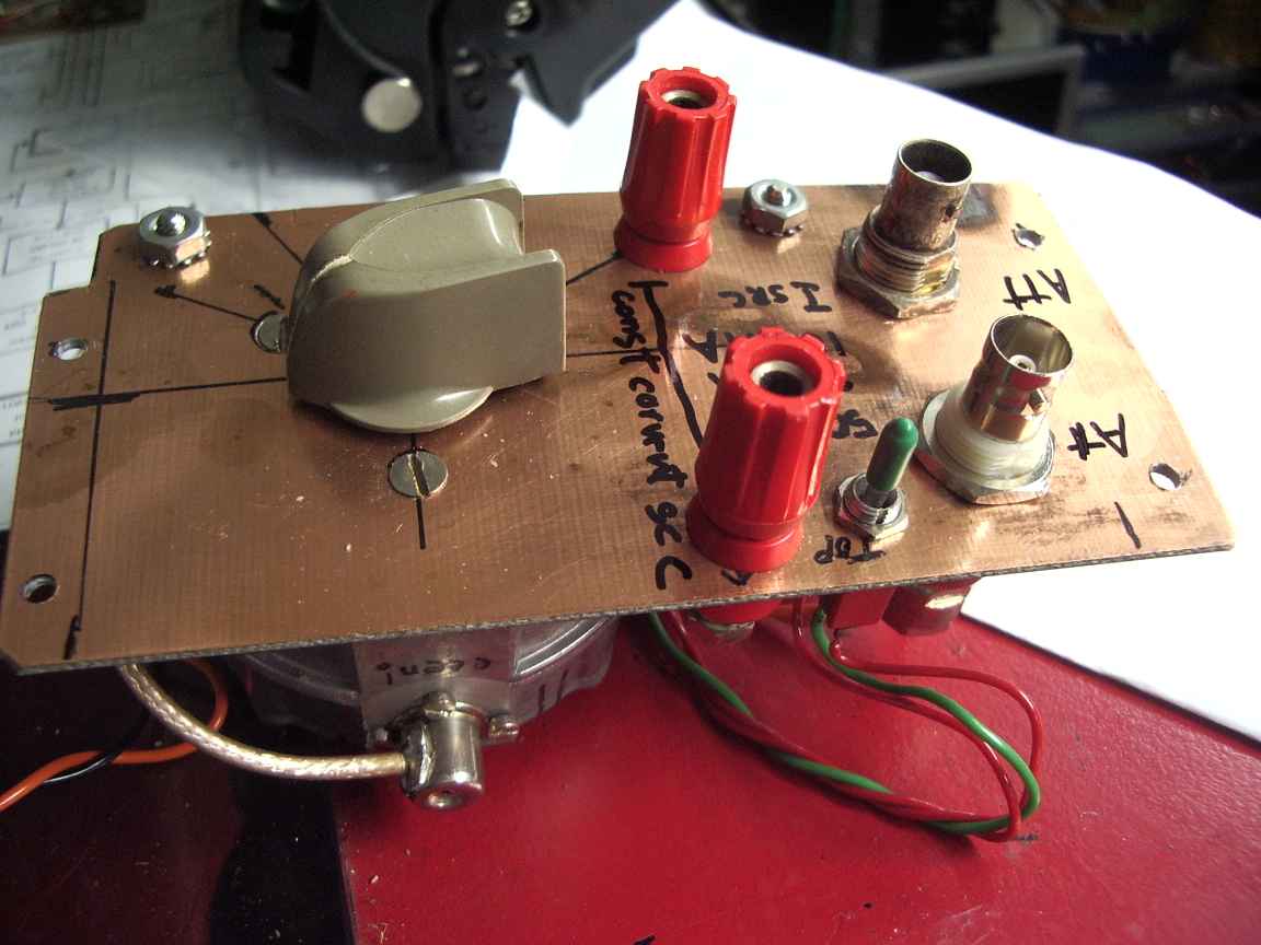
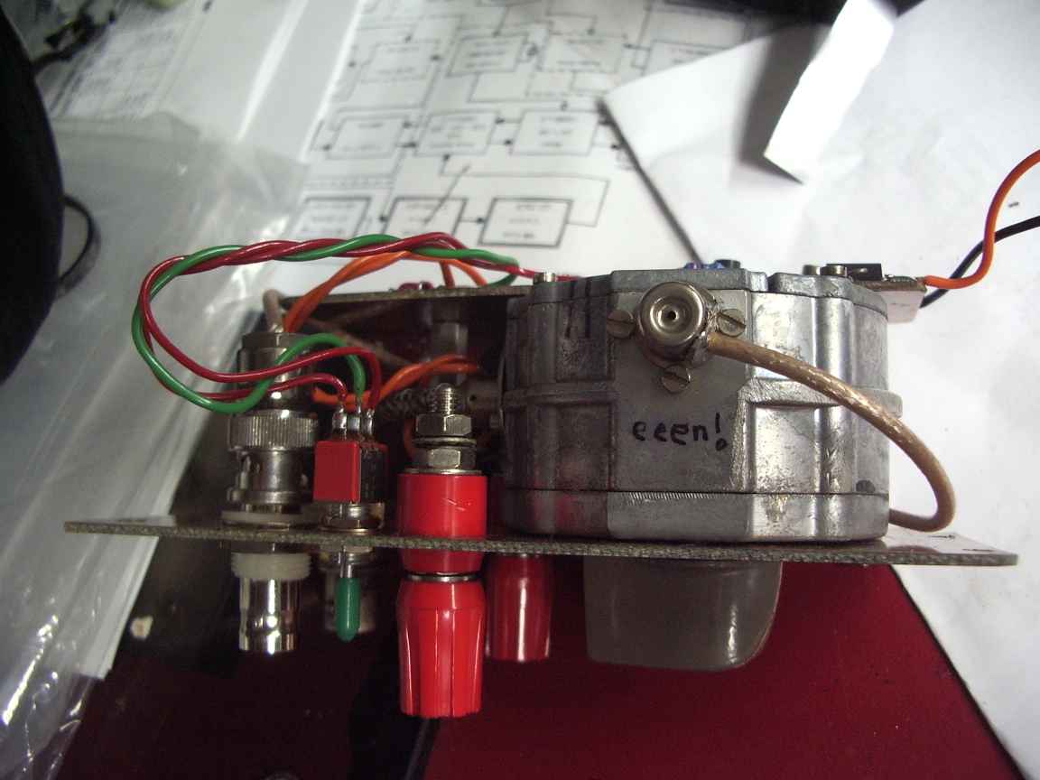
In my implementation the programming resistor is selected with a 3 position toggle switch to give 100mA, 50mA and 20mA.
